
An implementation of an I2C interface on the Lattice ICE40 LP8K. The project consists of a TinyFPGA BX and Raspberry Pi Zero W.
I set out to design a solid-state MFM hard drive clone knowing that much would need to be learned. I stumbled across a YouTube video titled Please electronic hobbyists… start using FPGA’s! It seemed a desperate plea. This led me to poke around and I quickly realized the FPGA would solve much of my project’s needs.
In this article we will focus on the Lattice ICE40 LP8K using the TinyFPGA BX board. The FPGA circuit will be designed in Icestudio. A Raspberry Pi Zero W will be used to test the circuit and will be coded in Java using NetBeans 10.0 and use the pi4j wiring library.
We won’t go into the detail of I2C here. You can find more information on the subject from Wikipedia. Suffice it to say that I2C is a fast, 2-wire, serial protocol. It is ideal where high-speed communication with a minimum of connections is needed. I2C enables multiple devices to share the same connections where each device has a unique address.
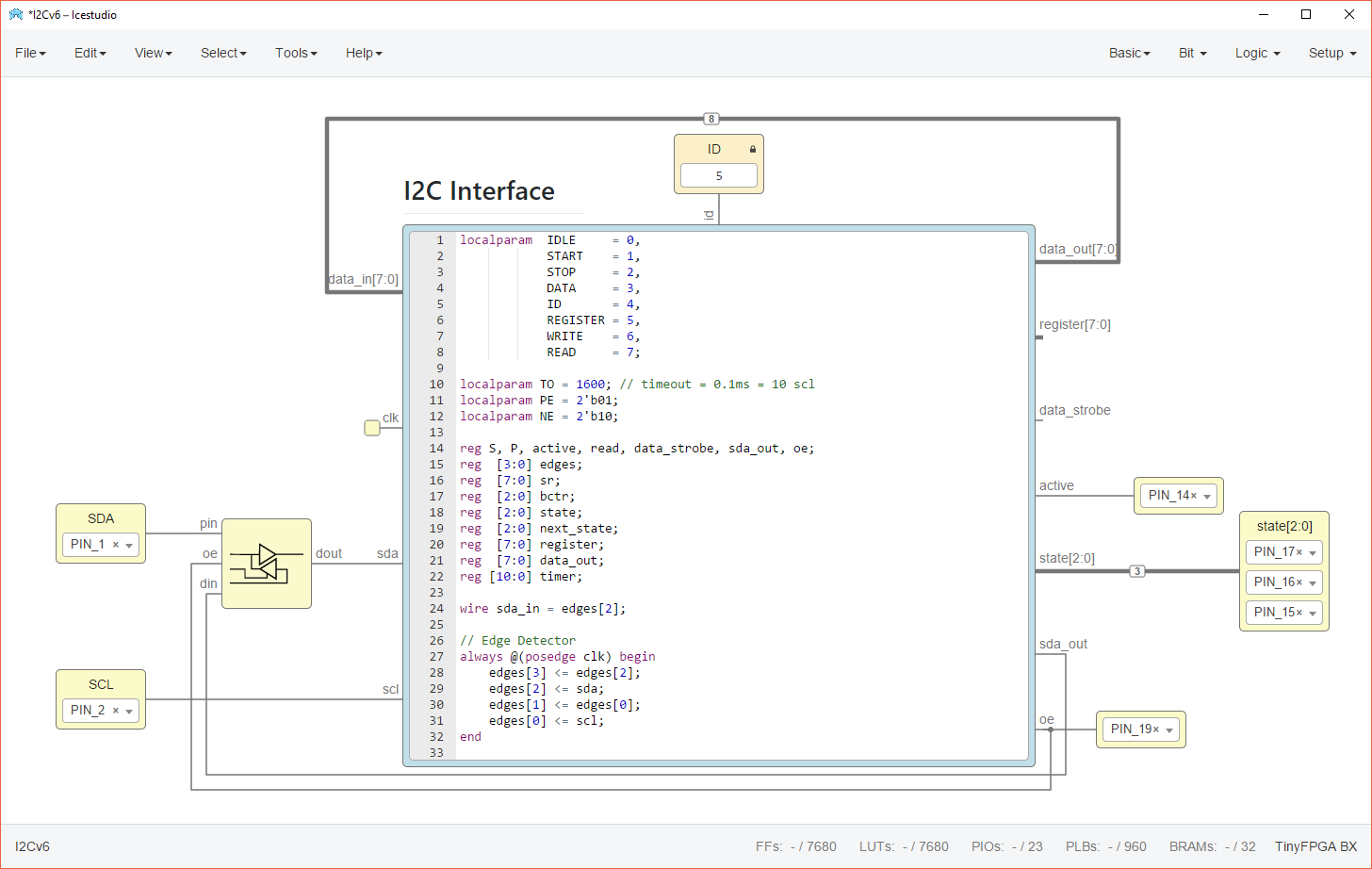
The I2C slave implementation consists of a bidirectional SDA data pin and SCL data clock pin. The design provides a parameter for setting the I2C address. The received data is looped back to the transmit data for immediate verification that the data was indeed received properly.
Because we are using Icestudio for this project, we will refer to code block inputs and outputs as module inputs and outputs.
The FPGA design requires signal edge detection to detect start and stop signaling of the master device. Lattice ICE40 devices do not provide edge detection for I-O pins so we will discuss this first. We will then continue with the state machine which controls the I2C functionality.
Edge Detection
Edge detection is accomplished by using a 4-bit shift register. Actually it is two 2-but shift registers assembled in such a way to make it easy to detect I2C start and stop states.
reg [3:0] edges;
On each FPGA clock, the I2C signals of SDA and SCL are registered in the edges register. In tandem, the previous values are shifted left. sda and scl are module (code block) outputs.
// Edge Detector
always @(posedge clk) begin
     edges[3] <= edges[2];
     edges[2] <= sda;
     edges[1] <= edges[0];
     edges[0] <= scl;
 end
Start (S) and stop (P) conditions are detected by checking the 4-bit register. Additionally, a register (active) is also set according to the start and stop conditions to indicate an active transmission. active is a module output.
reg S, P, active, ...

// Start-Stop Detector
always @(posedge clk) begin
     // Start Detector
     if (edges == 4'b1011) begin
         S <= 1;
         active <= 1;
     end
     else
         S <= 0;
     // Stop Detector
     if (edges == 4'b0111) begin
         P <= 1;
         active <= 0;
     end
     else
         P <= 0;
 end
State Machine
It took several weeks for me to arrive at a working state machine. Most of my efforts was in understanding the ICE40 behavior and Verilog HDL. After I became comfortable with both, I had trouble visualizing the state machine. Eventually, I found a simple spreadsheet was well suited to realize all of the states needed and to reduce the definitions required.
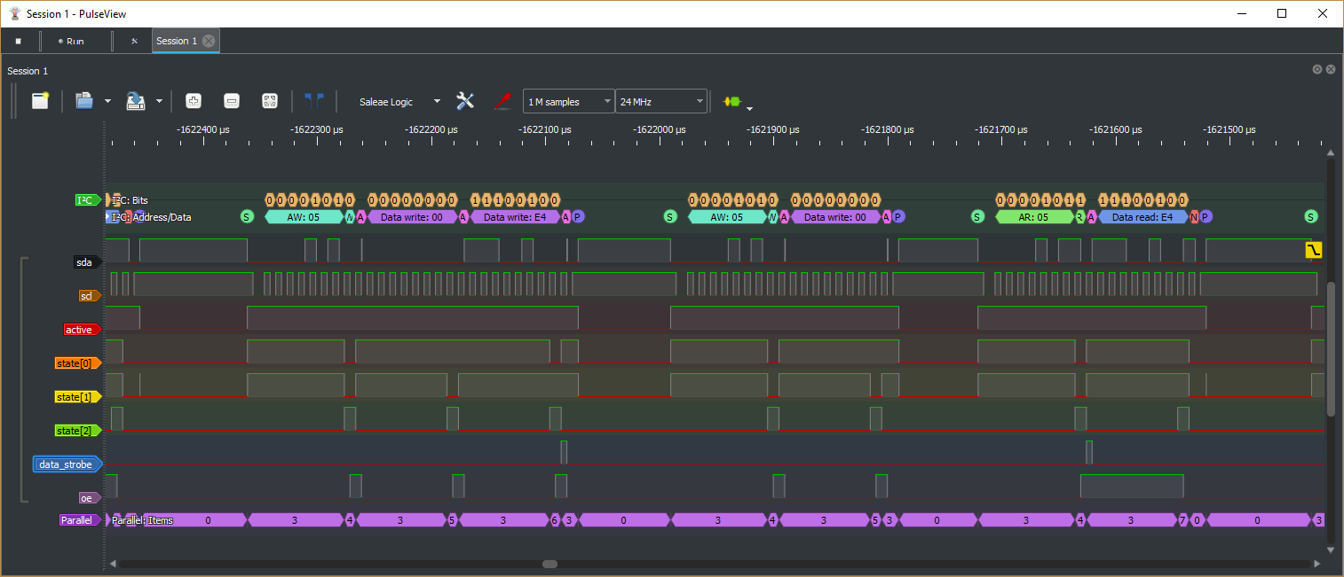
A very common use of I2C has two functions: read and write. Writing is performed by sending the 7-bit address including a read/write bit (set to ‘0’ indicating a write condition) followed by an 8-bit register address and then one or more data bytes to write to that register address. Reading is similar in that first the address byte with read/write bit set to ‘0’ and then the register byte is sent. A start sequence is sent again, called a restart and denoted as Sr. Then the address is sent again but this time with the read/write bit set to ‘1’. The I2C master then listens to the SDA line until the slave responds with NACK indicating the end of the stream or the master has read all it needs.
There are many ways to implement the I2C protocol. This is just one way. Exploring I2C device datasheets will demonstrate the flexibility of the protocol.
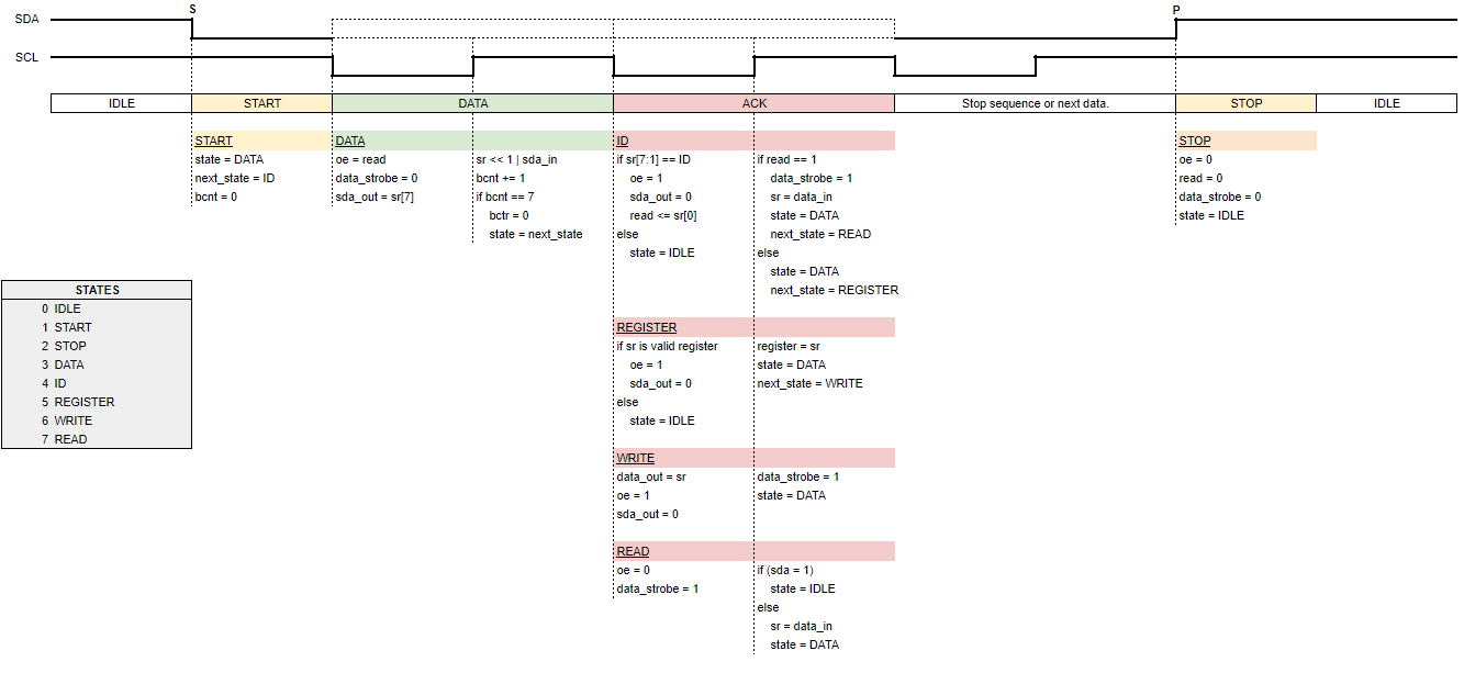
The states can divided in to two kinds: primary states and next states. Primary states are easily seen in the state logic diagram as IDLE, START, DATA, ACK and STOP. They are related to time based on the clock SCL. Next states are the activities that are performed that are specific to the bytes contained in the bit stream and include ID, REGISTER, WRITE and READ.
Each state may have a function to perform on the rising and/or falling edge of SCL.
START is activated when the start sequence S is detected. As a rule, SDA transitions occur only while SCL is logic ‘0’. Therefore, an SDA transition during the logic ‘1’ period of SCL signals an S or P condition. It is S when SDA falls and P when SDA rises during the positive period of SCL.
The address of the device intended to receive the message is then streamed from the master. Having just entered the START state, the slave will hold as its next state as ID while setting the primary state to DATA. After receiving eight bits of data the slave will parse and validate the address. If the address matches that of the id parameter, the slave will set the read/write bit as transmitted from the master. If the address is not of the slave, the state will be set to STOP wherein the slave will do a little cleanup and enter IDLE state.
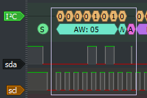
The ID state occurs during the ACK phase of the I2C stream. If the address received is of the slave, it will switch the SDA signal from an input to an output and hold the SDA signal to a logic ‘0’ for the duration of the SCL cycle within the ACK period. One of two next states may occur at this time: a read or write operation.
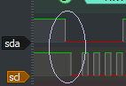
Note the little spike in the ACK phase in the image above. That is the transition of SDA from input to output. This does not pose a problem since the master will sample the ACK at the positive edge of the SCL. The same is true of all bits in the stream in that data is sampled at the positive edge of the stream.
In the more common implementations of I2C, to read or write a register is first addressed before performing the operation. So, if the read/write bit is a logic ‘0’, the master will apparently continue the stream and address the register. The slave will set its next state to REGISTER and primary state to DATA.

The slave will continue to receive eight more bits of data and at the ACK phase of the stream, store the register address. This particular implementation does not perform a validation of the register address but it could easily be incorporated.
If the master intends to continue to write data to this register address, it will continue to send one or more bytes of data until it is finished or the slave returns a NACK signal. That is, a logic ‘1’ during the ACK phase. In either case, once complete, the master will send a stop sequence and the slave will enter STOP state followed by IDLE state. The handling of received data following the REGISTER state will be performed by the WRITE state during the ACK phase of the stream.
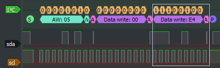
If the master intends to write to this register address, it will end the stream by sending a stop sequence after the ACK phase and reinitiate communications again.
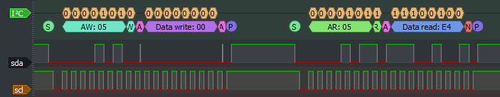
In the image above the master sends a stream of two bytes containing the slave and register addresses with the read/write bit as a logic ‘0’. The master ends transmission by sending the stop sequence and begins transmission again transmitting the slave address but with the read/write bit set to logic ‘1’ indicating a read stream. The slave reverses the dialog by setting the SDA signal from input to output and transmits data to the master.
In read mode, the slave monitors the ACK phase. The master will respond with an ACK (logic ‘0’) if it wishes to continue receiving the next byte or a NACK (logic’1′) to signal the end of read operations. When the slave receives a NACK, it will transition to STOP and then IDLE states. Read data will be handled by the READ state during the ACK phase of the stream following the REGISTER state.
Timeout
One more feature of this implementation is a timeout function. If the slave is active and a period of ten SCL clocks transpires, the timeout timer will set state to STOP.
localparam TO = 1600; // timeout = 0.1ms = 10 scl

reg [10:0] timer;

always @(posedge clk) begin

// Timeout timer
     if (active && (edges[1:0] == PE))
         timer <= 0;
     else begin
         timer <= timer + 1;
         if (timer > TO)
             state <= STOP;
     end
end
Java
package fpga.i2c;

import com.pi4j.io.i2c.I2CBus;
import com.pi4j.io.i2c.I2CDevice;
import com.pi4j.io.i2c.I2CFactory;
import com.pi4j.util.ConsoleColor;
import java.io.File;
import java.io.IOException;

public class Main {

    public static void main(String[] args) throws
            InterruptedException,
            IOException,
            I2CFactory.UnsupportedBusNumberException {

        System.out.println("begin.");

        // Connect to I2C bus 1
        I2CBus i2c = I2CFactory.getInstance(I2CBus.BUS_1);

        // Create device object
        I2CDevice device = i2c.getDevice(5);

        byte[] buffer = new byte[2];

        while (true) {
            try {
                for (int i = 0; i < 256; i++) {
                    device.write(0, (byte)i);
                    device.read(0, buffer, 0, 1);
                }
            } catch (Exception e) {

            }
            Thread.sleep(1);
        }
    }
}
1 thought on “An I2C slave on an ICE40 FPGA”
Rick MacDonald September 27, 2019 at 10:15 am
Great article Chris and exactly what I was looking for! One thing I would like to point out to anyone else who is interested in this is that if you try to write to registers 6 or greater it will fail. This made me scratch my head but eventually I realized that the behavior is exactly what the Verilog code implements but you didn’t mention that in the article. No problem and mystery solved.
Reply